
CHA/V 2.0 Build Guide
Hello! Thanks for coming on this crazy journey with me.
Below is a link to a PDF document with all the parts you’ll need. Almost everything can be purchased from Tayda. I recommend Tayda for beginners because they’re relatively inexpensive and the site is easy to navigate. Tayda part numbers are listed for each part and can be copied and pasted into the search bar. Parts with recommended upgrades not available from Tayda are marked with an asterisk. Ali Express is another source for getting things cheaply, although quality is sometimes an issue, and shipping from Asia is usually slow and unpredictable.
Other things you’ll need not mentioned in the BOM:
— hook up wire. I recommend 22AWG stranded wire. The little kits you can get with multiple colors are nice to have. If you don’t forsee a lot of synth DIY in your future, you can buy small amounts of wire from Tayda for $0.10 per ft. You can get a few feet of just one color if you’re hardcore, but I’d recommend that you get 1ft. of each color they have. Red, Green, Blue, Yellow, White, Black.
– a 12v center positive wall wart. 500mA is plenty, and you can get away with less. Jameco is a good source for these in the US. Before you buy one, look through what you already have. 12v center positive is pretty common. You probably already have one. You can also power a CHA/V with a 9v battery. The signal will be slightly cleaner, and not quite as bright.
All said and done, and including the PCB, the parts will probably cost you less than $50.
Build Guide
OK, here we go! After helping hundreds of people make these things, I’ve seen this be pretty easy build for anyone with a bit of soldering experience. I’d recommend skimming the guide even if you’re experienced though. There are some counterintuitive bits that can be made much easier with a few tricks I’ve outlined here.
For those of you that are new to soldering, this is a difficult but possible beginner project. I’ve watched many people who had never soldered anything before make these. Most of the parts are resilient, and other than the switches, you probably won’t kill anything by overheating it. The printed circuit boards however are purposely inexpensive, and hammering on a single pad with a hot soldering iron for more than 10 or 15 seconds could potentially cause some damage.
With some decent quality solder (I like Kester 24-6040-0027) each solder joint should only take 2-3 seconds to make. 60/40 solder contains lead, but as long as you don’t eat any and you wash your hands when you’re finished, the chances of it harming you in any way are probably infinitesimal.
If you’re struggling with a particular part, take a break, take a breath, and come back to it later. Take your time, stay positive, and message me if you’re really stuck. We’ll get through it.
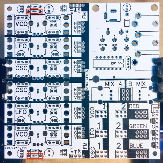
Step 1: Solder in the 100k resistors. Resistors aren’t “polar”, so there isn’t a right or wrong direction to place them in.
The 100k resistors are part of the LED driver circuit for VCO1 and VCO2. They attenuate incoming voltage to the transistors that drive the LEDs.
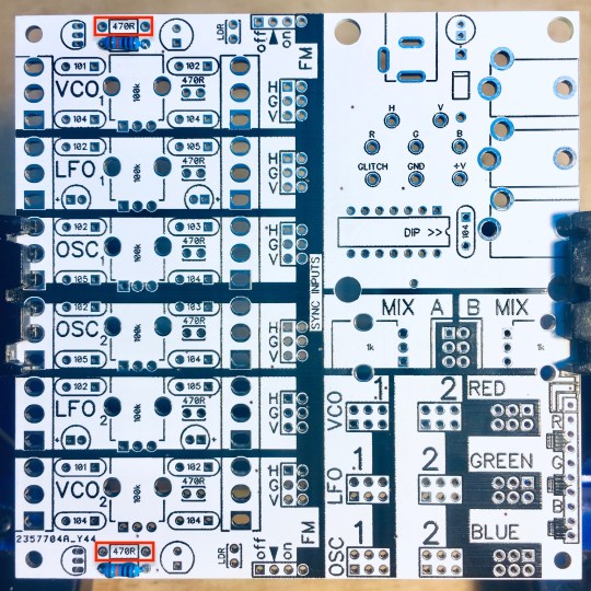
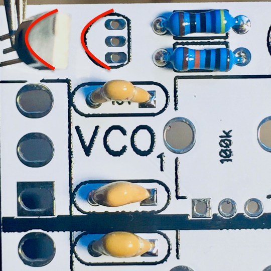
Step 2: Solder in 2 of the 470R resistors as shown. Put the rest of them away for now. Trust me. Put them away.
The 470R resistors limit the current to the LEDs, keeping them from burning up and also determining the maximum brightness. Higher resistance would make them dimmer, and lower resistance would make them brighter. You can experiment with the values if you want, but I wouldn’t recommend going lower than 220R.
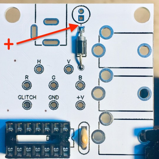
Step 3: Solder in the 4001 rectifier diode. Diodes are “polar”, meaning there’s a right way and a wrong way to install them. Line up the stripe on the diode with the stripe in the picture and you’re good to go.
Rectifier diodes are like one-way valves that only allow current to flow from the anode to the cathode. In this circuit, the 4001 is being used to protect the power inlet from reverse polarity. If you accidentally use a center negative power supply instead of center positive, the 4001 will theoretically block the negative current, protecting the chips and electrolytic capacitors from being destroyed.

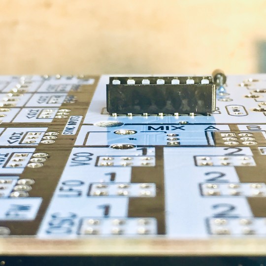
Step 4: Place the IC socket on the board, but don’t solder it in yet. The socket has a little indentation on one end that tells you which way to place it. If you happen to solder it in backwards, it doesn’t matter as long as you don’t also put the chip in backwards.
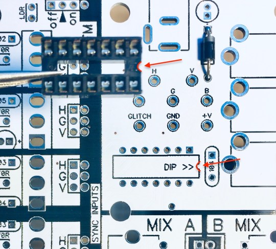
Step 5: Flip the board over and tack one leg of the IC socket.

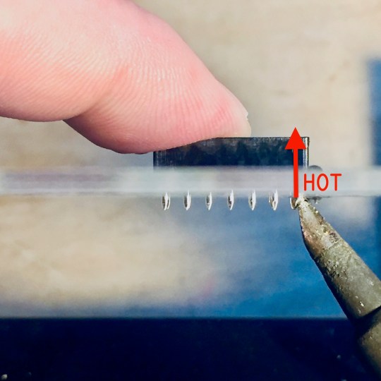
Step 6: If the socket is nice and flat against the board, you can go ahead and solder the rest of the pins. If not, we’re going to use a technique that we’ll also use later on the pin headers and switches. Heat the pin that you tacked before and at the same time, gently press down on the socket with your finger until it’s flat against the board. Keep in mind which pin you’re heating and keep your finger away from it — it will be hot enough to burn you if you touch it.
Step 7: Once the socket is nice and flat against the board (as shown) you can solder all the pins. Reflow the solder on the one you tacked, but not until all the other pins are soldered. Having a crooked socket won’t affect the functionality, but getting it straight is good practice for all the pin headers and switches we’re gonna do later.
Step 8: We’re about to do all the MLCC capacitors (they aren’t polar). The codes are all printed on the PCB to make things a little quicker and easier (as shown with the 100pF caps below). Also, here’s a handy little decade capacitor conversion chart:


Step 9: Solder in the two 100pF capacitors.
Each of the six oscillators has four capacitors that can be selected with switches. The two on the left are to select timing. The top is for higher frequency, and the bottom is for lower frequency. The two on the right are to select AC coupling and filtering. The top one makes thinner lines and works better with the high timing capacitor, while the bottom one make thicker lines and works better with the low timing capacitor.
The 100pF capacitors you just soldered in have the lowest capacitance in this project, and therefore produce the highest frequencies. They’re used as the high-frequency timing caps for the VCOs (voltage controlled oscillators). As video oscillators, they will produce oscillations that are capable of making lots of vertical lines that are much too high-frequency to hear.

Step 10: Solder in the six 1000pF capacitors.
The 1000pF capacitors are used for high-frequency timing in the LFOs (low frequency oscillators) and utility oscillators (OSC 1&2). 1000pF is still very fast, just not quite as fast as the VCOs — they allow us to get a slightly lower frequency range that is still useful for vertical lines but gives us some variety. 1000pF is also used for the high (thin-lines) coupling caps in the VCOs.

Step 11: Solder in the two 0.01uF capacitors.
The 0.01uF caps are used as the high coupling caps for the OSCs.

Step 12: Solder in the seven 0.1uF caps.
The 0.1uF caps are used as low-frequency timing caps in the VCOs. These will give us some nice horizontal lines that are audible. They’re also used as low coupling in the VCOs and OSCs.
There’s another 0.1uF next to the IC socket. 0.1uF is typically used as a “bypass” capacitor for chips. One leg is connected to the +V input of the chip, and the other leg is connected to ground. The purpose of bypass capacitors is to provide clean power to chips by shorting some of the noise to ground.
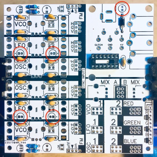
Step 13: Solder in the four 1uF caps. These are the last of the MLCC caps.
You’re getting the hang of this! 1uF is used as low timing for the OSCs, and high coupling for the LFOs.

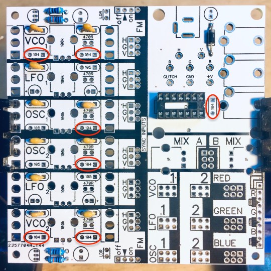
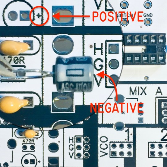
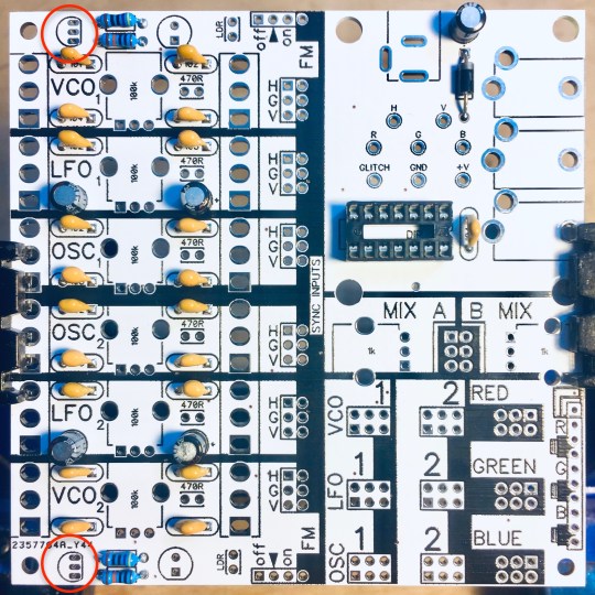
Step 14: Ok, time for the 10uF electrolytic capacitors. These are polar, and they will potentially explode if you put them in backwards. If you’re experienced at this, you’ve probably taken one to the face and then screamed like a 5-year-old (like I have) so bear with me while I explain this to the new people.
The PCB has little plus sign markings to show you where the positive leg goes, and electrolytic capacitors usually have a stripe with a minus sign to show you where the negative leg is. In the picture, you can see the stripe on the negative side and a little rectangular minus sign. Don’t solder these in just yet..
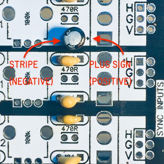
Below is what the 10uF caps will look like when they’re soldered in correctly. The stripe (negative leg) is facing away from the plus sign on the PCB. Hold your fire though — there’s another important thing..
The little plus sign for this one got eroded away by the rectifier pad (sorry). That tiny speck on the board was supposed to be a plus sign. One more thing before you start soldering..
If you got the 5mm electrolytics from Mouser or LCSC, you can go ahead and solder them in. Just make sure the stripe is facing away from the rectifier like in the picture. If you have the tall electrolytics from Tayda, wait a second and look at the next picture.
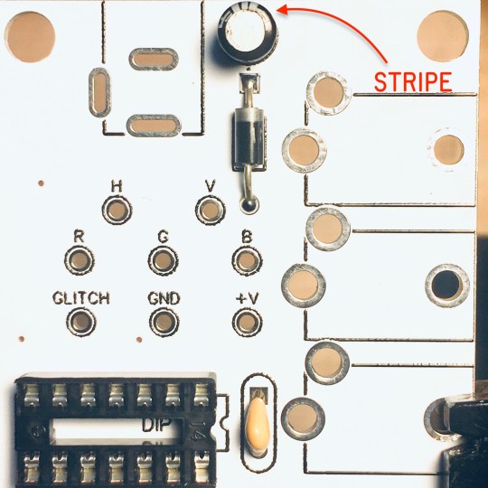
The VGA test board is eventually going to go on top of this area, and the Tayda capacitors will be too tall. The rest of the electrolytics can stand up (they’re fine — just a little annoying in my opinion) but this one needs to be bent to the side. Bend the legs before installing it and then solder it in. Again, make sure the stripe is facing away from the rectifier diode.
10uF is a typical capacitor value for filtering noise from the power supply. The +V from the rectifier diode is connected to the + leg of the capacitor, and the – leg of the capacitor goes to ground. This filters out some of the noise from the power supply and keeps it out of the oscillators.

OK, you’ve been very patient, lol. Get all those 10uFs in now.
10uF is used for low timing and low coupling in the LFOs. 10uF will give us a range that goes from sub-audio (just an intermittent click and flash of color) to audio rate that produces a tone and thick horizontal lines.
Step 15: Solder in the two 2n3904 transistors. Transistors can be overheated, so take it easy on them. More than 5 seconds on a single leg probably isn’t a great idea. Also, it’s easy to accidentally bridge the pads when you’re soldering transistors, so make sure the tip of your soldering iron is clean. There’s no need to panic, just try to do it neatly.
The transistors are part of the LED driver circuitry. A signal applied to the FM pin goes through an attenuator formed by the 100k resistor into the base of the transistor, allowing current to flow through the LED. This is a common LED driver circuit.
You probably knew this (or figured it out), but there’s a right way and wrong way to put the transistors in. Make sure the curved sides on the transistors are oriented with the curved sides on the PCB markings.
Step 16: We’re going to put in the LEDs and LDRs now, but please read ahead before you solder them in.

It’s really tough to see on 3mm LEDs, but LEDs typically have a round side and a flat edge. The flat edge (99% of the time) is the cathode and has a shorter leg. Orient the the flat edge of the LED with the flat edge of the PCB marking. Don’t solder it in quite yet.
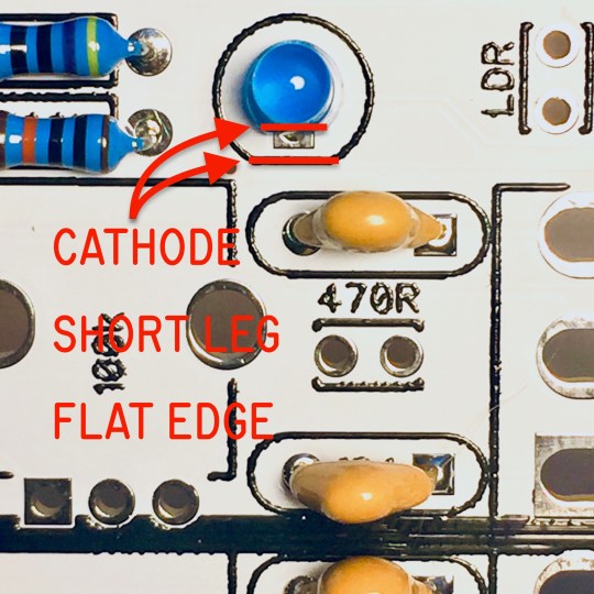
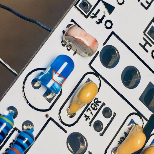
We’re going to bend the LED and the LDR legs to right angles so they face each other. This is a little easier if you bend the legs before you place them in the board. I’ve traced the little anvil shape on the LED in the picture below. This is the fail-safe way to identify the LED cathode. The anode has a little post, and the cathode has a big anvil. LDRs (light dependent resistors) aren’t polar.
An LED and LDR facing each other like this are called a vactrol. LDRs change resistance based on how much light they can see. When an LED shines directly in their eyes, their resistance drops. This is a hacky way to make a voltage controlled resistor. When we add them into our oscillator circuit, the vactrol can be used to animate the frequency of the oscillator. If we route a signal through the LDR, the vactrol can be used as a voltage controlled attenuator. If you’d like, you can use heat shrink or electrical tape to block ambient light, so the LDR can only see the LED. You can also buy factory made vactrols, but they tend to be expensive. I prefer to leave the LDRs out in the open so that they can also be played like a pseudo theremin.
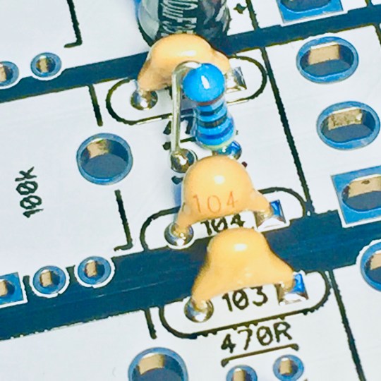
Step 17: Remember those 470R resistors? Ok, it’s time to bring them back. They’re going to be vertically mounted, so bend them like the picture below.

Each of the oscillators gets a 470R resistor.

This is how they look when they’re soldered in (below).
The 470R resistors provide a minimum resistance in the oscillator circuit. They’re placed in series with the 100k potentiometers. Without these resistors, it would be possible to have 0 resistance in the schmitt-trigger oscillator feedback loop, which is fine for an audio oscillator, but can cause problems when the oscillators are synced to video. When the oscillators are synced to video, 0 resistance in the feedback loop would allow the VGA sync to be shorted to ground, causing the output signal to crash.
Step 18: Ok, now we’re going to put in lots of pin headers. If you were a novice at soldering before this project, you’re about to become an intermediate. The first one is the 3×2 pin header row shown below. Before doing any of this, I’d recommend watching all three of the pin header videos below (pt. 1-3).

If you decide to make the easy headers, you’ll need 5 of them. Place them in the spaces below. If you’re feeling saucy, you can just do 3×2 rows, and then you’ll need a total of 16. Try to keep these neat and straight — these will be your patch points (more on this in the user guide), and they will be easier and more pleasant to use if you keep them tidy.

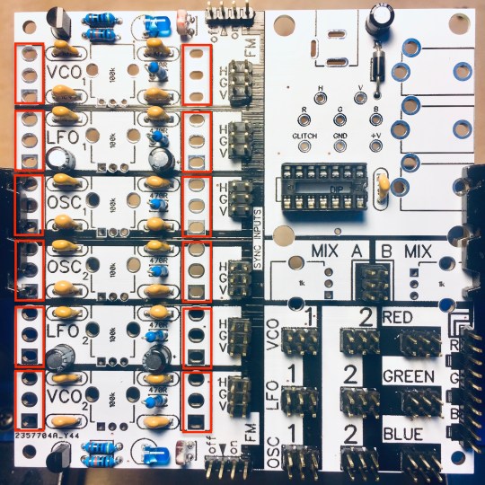
You can break the single row pin headers with your hands. Just grasp them firmly and snap them (or clip them with flush cutters if you insist). You’ll need two 4×1 rows, and one 10×1 row.
The 4×1 rows are for patching the LED driver circuits. The 10×1 row is for patching the 3.5mm jacks to get audio in or out, or to interface with a modular synthesizer.

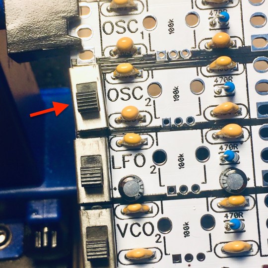
Step 19: Now it’s time for the switches. Switches are notorious for failing when they’re overheated, so take it easy on them. They’re also tricky to get in straight, so I’d recommend tacking the center pin and then checking to make sure the switch is lined up properly before soldering the other two pins. Below is a picture of a crooked switch, which is a bummer, but luckily only the center pin has been tacked, so it can be moved back into place easily using the same trick we used on the socket and pin headers. Go easy on the heat though. When soldering switches, apply heat with the iron, count 2 seconds, and then add the solder for 1 second. If it takes longer, stop and let the parts cool completely before trying again.
The 12 switches go in these places (below).
The row of switches on the left select the timing capacitors for each oscillator (low/high frequency). The row of switches on the right select the coupling/filter capacitors for each oscillator (thick/thin).
Step 20: Finally, a fun and easy part. It’s time for the potentiometers. There are two values of potentiometers in this project, so don’t accidentally mix them up. The six 100k potentiometers go here (below).
The 100k potentiometers set the frequency for each oscillator.

Step 21: Now for the two 1k potentiometers. They go here (below).
The 1k potentiometers are connected to the 3×2 pin header. Each one is an independent, patchable “dirty mixer”. The dirty mixer is a simple circuit invented by the video artist Karl Klomp initially as conceptual art. In the CHA/V, dirty mixers have many practical uses (covered in the user guide).

Step 22: Ok, almost done! You might be tempted to go ahead and put in the rest of the parts on the board. Trust me, do not. Things will be considerably more difficult if you do. Put the PCB aside for a moment. If you’re tired at all, this might be a good time for a break, or even to call it a day. The next bit is the hardest part.

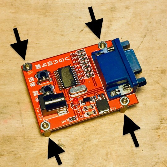
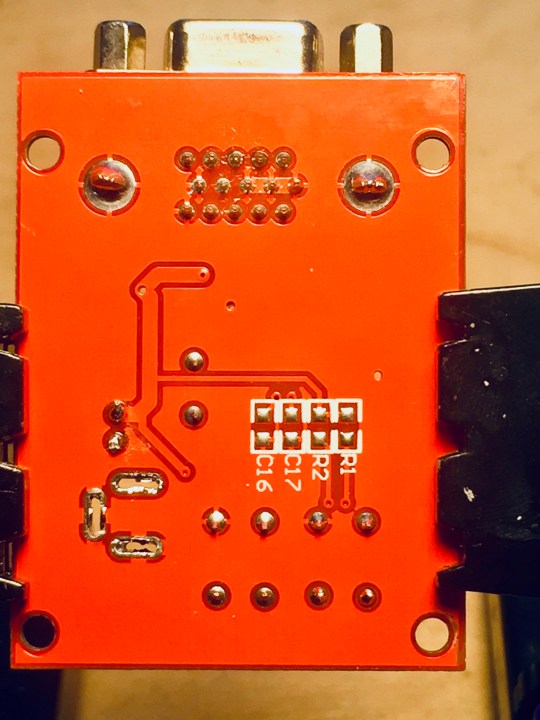
Step 23: Remove the four stand-offs from the VGA test signal generator and set them aside. We’re going to use them later.
Optional: As long as we’re hacking the VGA tester, might as well put the LED in all the way. Whoever builds these at the factory always leaves them sticking out really far. Can’t blame them — it’s probably not the most pleasant job. In my builds, I usually just pull them out and replace them with a different color for style points.

Optional: Remove the DC power jack from the VGA tester. If you bought an extra one, this is optional, and you might want to do it just for aesthetics. If you didn’t buy an extra one, this isn’t optional. How to vid below:
If the flux snot (below) bothers you..
..you can clean it with some 99% IPA and wipes. The things I like to use are below:
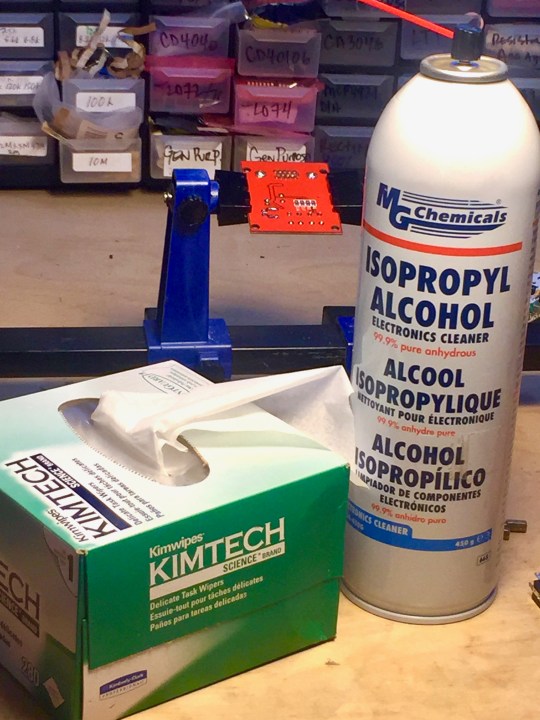
ALL CLEAN!
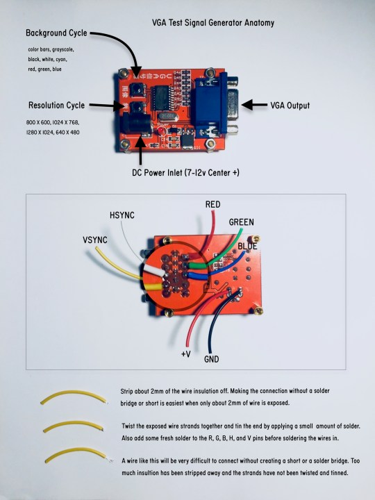
Step 24: Prepare for the hardest part of the whole build. This is the original hack that started the whole CHA/V movement. We’re going to add wires to the VGA tester pins. The colors don’t matter — you can use all the same color if you want — it’s just much easier to keep things organized when they’re color coded. Watch the wiring vids (pt. 5 and pt. 6) below before you try it.

Here’s the handout I made for workshops if you’d like to see a different view of that.
Step 25: You’re in the eye of the storm. Using four M3 nuts, put the 10mm stand-offs in where the 8mm ones used to be. Make sure to add the washers. 10mm stand-offs with washers will give you the perfect height to clear the DC jack once it’s soldered to the CHA/V PCB.
Step 26: Install the chip. Here’s a little trick to make it easier:
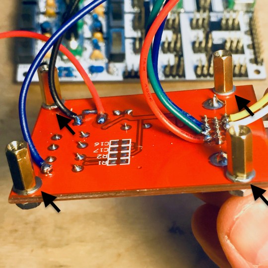
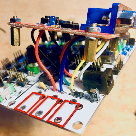
Step 27: Getting there. This is the last tricky part. We have to use the wires we installed to connect the VGA tester to the CHA/V PCB. Watch the vids pt. 8, 9, and 10 for the least painful way I’ve found to approach this.
Note: If any of your wires fall off or break off during this process, consider it a blessing. What this means is that they weren’t on good enough in the first place, and they failed at a time when you could diagnose and repair them easily.
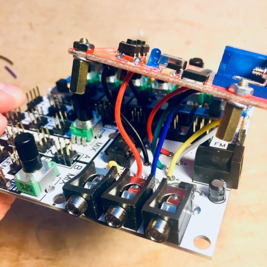
Step 28: Now that all the wiring is done, we can install the DC jack. Easy peasy.

Step 29: Home stretch, the three 3.5mm jacks.
A L L T H E S O L D E R I N G I S D O N E ! ! !
consider yourself a hero.
Step 30: Make the sandwich. Watch the pt. 11, the final installment. In the video, I ran out of washers for the 8mm standoffs, but you should have 4 extra ones — use ’em.
YOU DID IT! YOU ARE A DIY ELECTRONICS WARRIOR! NOW GO EAT A SANDWICH 😉
(but wash your hands first, especially if you were using leaded solder)
