
CHA/V 3.0 Build Guide
[under construction]
Welcome to the world of hacky video synthesis!
There are two options for parts depending on how you’re going to build.
Click on the link below that describes your build to automatically download a Word document of the parts list for you (check your downloads folder after you click).
The lists contain “Quick Order” instructions for painless automated ordering from Tayda.com.
I’m going to build both VGA4EVA and CHA/v 3.0 (only order this list once if you’re building both)
I’m going to source my own VGA Test Signal Generator and build a CHA/V using that instead of VGA4EVA
If you’re building VGA4EVA along with a CHA/V 3.0, I’d recommend starting with VGA4EVA. It’s the easier of the two builds, and it can do a few things without the CHA/V. Once it’s up and running, you can add the CHA/V.
One day there might be a dedicated 3.0 build guide, but in the meantime:
CHA/V 3.0 was almost a total re-design in terms of circuit routing on the board, but it’s almost identical to CHA/V 2.0 on the surface, so much so that you can use the CHA/V 2.0 Build Guide for almost the entire build. In fact, if you’re building your CHA/V 3.0 using a VGA Test Signal Generator that you sourced, you can follow the entire 2.0 guide. The rectifier diode and power capacitor moved, but you can follow the directions anyway — just put them in their new places instead.
If you built a VGA4EVA and you’re ready to add the CHA/V, you can also use the CHA/V 2.0 Build Guide for now. Here are some instructions:
1. You can ignore all the stuff in the beginning. Just start with Step 1.
2. Don’t install the rectifier diode in Step 3. The one in VGA4EVA is all you need, it’ll protect both devices.
3. Install the four 10uF capacitors on the LFOs according to the directions in Step 14, but hold off on the single 10uF capacitor in the power inlet section for now. There are some options about how to install it — you can install it normally, fold it over, or install it on the underside of the board.
4. Don’t install the 10×1 Pin Header Row in Step 18. It will also go on the underside of the board, and connect to VGA4EVA.
5. Come back here when you’ve gotten to Step 22.
6. Once Step 22 is done, install the 8×1 and 10×1 headers that will connect the two boards together.
The easiest way to do this is:
a) install the standoffs on VGA4EVA
b) break off a 8×1 pin-header row and a 10×1 pin header row and insert them into the 8×1 and 10×1 receptacle headers.
c) dry fit the headers
d) stack CHA/V on top of VGA4EVA, and make sure the header pins are all lined up with the PCB holes
e) solder them in place
NOTE: Make sure each of these pins has a good solder joint. It should be a shiny little Hershey’s kiss looking solder joint. After checking the power, these pin headers are my first destination on the troubleshooting tour when people write in looking for help. If they aren’t soldered correctly, things aren’t going to work.
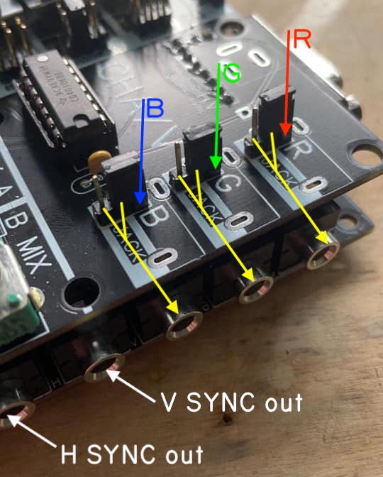
7. Break off three 3×1 pin header strips and install them as pictured below. These will be your headers for the assignable 3.5mm jacks.
DONE!
